Journals > > Topics > Special Issue on Metal Halide Perovskite and Their Applications
Special Issue on Metal Halide Perovskite and Their Applications|5 Article(s)
Stable and high performance all-inorganic perovskite light-emitting diodes with anti-solvent treatment|Editors' Pick
Sajid Hussain, Ahmad Raza, Fawad Saeed, Abida Perveen, Yan Sikhai, Nasrud Din, Elias E. Elemike, Qianqian Huang, Alagesan Subramanian, Qasim Khan, and Wei Lei
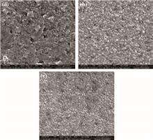
Optoelectronic applications based on the perovskites always face challenges due to the inherent chemical composition volatility of perovskite precursors. The efficiency of perovskite-based light-emitting diodes (Pe-LEDs) can be enhanced by improving the perovskite film via solvent engineering. A dual solvent post-treatment strategy was applied to the perovskite film, which provides a synchronous effect of passivating surface imperfections and reduces exciton quenching, as evidenced by improved surface morphology and photoluminance. Thus, the optimized Pe-LEDs reach 17,866 cd·m-2 maximum brightness, 45.8 cd·A-1 current efficiency, 8.3% external quantum efficiency, and relatively low turn-on voltage of 2.0 V. Herein, we present a simple technique for the fabrication of stable and efficient Pe-LEDs. Optoelectronic applications based on the perovskites always face challenges due to the inherent chemical composition volatility of perovskite precursors. The efficiency of perovskite-based light-emitting diodes (Pe-LEDs) can be enhanced by improving the perovskite film via solvent engineering. A dual solvent post-treatment strategy was applied to the perovskite film, which provides a synchronous effect of passivating surface imperfections and reduces exciton quenching, as evidenced by improved surface morphology and photoluminance. Thus, the optimized Pe-LEDs reach 17,866 cd·m-2 maximum brightness, 45.8 cd·A-1 current efficiency, 8.3% external quantum efficiency, and relatively low turn-on voltage of 2.0 V. Herein, we present a simple technique for the fabrication of stable and efficient Pe-LEDs.
Chinese Optics Letters
- Publication Date: Mar. 10, 2021
- Vol. 19, Issue 3, 030005 (2021)


Optoelectronic and elastic properties of metal halides double perovskites Cs2InBiX6 (X = F, Cl, Br, I)
Muhammad Saeed, Izaz Ul Haq, Shafiq Ur Rehman, Akbar Ali, Wajid Ali Shah, Zahid Ali, Qasim Khan, and Imad Khan
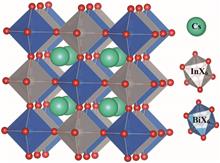
Structural geometry, electronic band gaps, density of states, optical and mechanical properties of double perovskite halides Cs2InBiX6 (X = F, Cl, Br, I) are investigated using the density functional theory. These compounds possess genuine perovskite stoichiometry, evaluated using various geometry-based indices like tolerance factor, octahedral factor, and formation energy. The fundamental electronic band gaps are direct and valued in the range 0.80–2.79 eV. These compounds have narrow band gaps (except Cs2InBiF6) due to strong orbital coupling of the cations. The valence band maximum and conduction band minimum are confirmed to be essentially of In 5s and Bi 6p characters, respectively. The splitting of Bi 6p bands due to strong spin-orbit coupling causes reduction in the band gaps. These compounds have large dispersion in their bands and very low carrier effective masses. The substitution of halogen atoms has great influence on the optical properties. The mechanical properties reveal that Cs2InBiX6 (X = F, Cl, Br, I) satisfy the stability criteria in cubic structures. Structural geometry, electronic band gaps, density of states, optical and mechanical properties of double perovskite halides Cs2InBiX6 (X = F, Cl, Br, I) are investigated using the density functional theory. These compounds possess genuine perovskite stoichiometry, evaluated using various geometry-based indices like tolerance factor, octahedral factor, and formation energy. The fundamental electronic band gaps are direct and valued in the range 0.80–2.79 eV. These compounds have narrow band gaps (except Cs2InBiF6) due to strong orbital coupling of the cations. The valence band maximum and conduction band minimum are confirmed to be essentially of In 5s and Bi 6p characters, respectively. The splitting of Bi 6p bands due to strong spin-orbit coupling causes reduction in the band gaps. These compounds have large dispersion in their bands and very low carrier effective masses. The substitution of halogen atoms has great influence on the optical properties. The mechanical properties reveal that Cs2InBiX6 (X = F, Cl, Br, I) satisfy the stability criteria in cubic structures.
Chinese Optics Letters
- Publication Date: Mar. 10, 2021
- Vol. 19, Issue 3, 030004 (2021)
High-brightness red-emitting double-perovskite phosphor Sr2LaTaO6:Eu3+ with high color purity and thermal stability [Invited]|On the Cover
Zongjie Zhang, Wei Li, Nan Ma, and Xiaoyong Huang
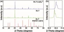
Bright Eu3+-activated double-perovskite Sr2LaTaO6 red-emitting phosphors were successfully synthesized by a high-temperature solid-state method. Under near-ultraviolet excitation at 394 nm, optimal Sr2LaTaO6:0.2Eu3+ phosphors emitted high-brightness red light around 613 nm with the International Commission on Illumination chromaticity coordinates (0.650, 0.349). Notably, the color purity can reach 92%. Impressively, the favorable thermal stability of the Sr2LaTaO6:0.2Eu3+ phosphors was characterized by temperature-dependent emission spectra at different temperatures from 303 to 463 K, and the emission intensity at 423 K remained 73% of its value at 303 K. All of the results suggested that the as-prepared Sr2LaTaO6:0.2Eu3+ phosphors can be used in near-ultraviolet-excitable white light-emitting diodes as a red-emitting color converter. Bright Eu3+-activated double-perovskite Sr2LaTaO6 red-emitting phosphors were successfully synthesized by a high-temperature solid-state method. Under near-ultraviolet excitation at 394 nm, optimal Sr2LaTaO6:0.2Eu3+ phosphors emitted high-brightness red light around 613 nm with the International Commission on Illumination chromaticity coordinates (0.650, 0.349). Notably, the color purity can reach 92%. Impressively, the favorable thermal stability of the Sr2LaTaO6:0.2Eu3+ phosphors was characterized by temperature-dependent emission spectra at different temperatures from 303 to 463 K, and the emission intensity at 423 K remained 73% of its value at 303 K. All of the results suggested that the as-prepared Sr2LaTaO6:0.2Eu3+ phosphors can be used in near-ultraviolet-excitable white light-emitting diodes as a red-emitting color converter.
Chinese Optics Letters
- Publication Date: Mar. 10, 2021
- Vol. 19, Issue 3, 030003 (2021)
Electron-beam-induced degradation of halide-perovskite-related semiconductor nanomaterials
Zhiya Dang, Yuqing Luo, Xue-Sen Wang, Muhammad Imran, and Pingqi Gao
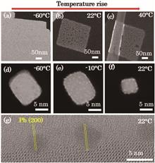
The instability of lead halide perovskites in various application-related conditions is a key challenge to be resolved. We investigated the formation of metal nanoparticles during transmission electron microscopy (TEM) imaging of perovskite-related metal halide compounds. The metal nanoparticle formation on these materials originates from stimulated desorption of halogen under electron beams and subsequent aggregation of metal atoms. Based on shared mechanisms, the TEM-based degradation test can help to evaluate the material stability against light irradiation. The instability of lead halide perovskites in various application-related conditions is a key challenge to be resolved. We investigated the formation of metal nanoparticles during transmission electron microscopy (TEM) imaging of perovskite-related metal halide compounds. The metal nanoparticle formation on these materials originates from stimulated desorption of halogen under electron beams and subsequent aggregation of metal atoms. Based on shared mechanisms, the TEM-based degradation test can help to evaluate the material stability against light irradiation.
Chinese Optics Letters
- Publication Date: Mar. 10, 2021
- Vol. 19, Issue 3, 030002 (2021)
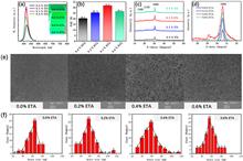
Interface and bulk controlled perovskite nanocrystal growth for high brightness light-emitting diodes [Invited]
Le Jiang, Xi Luo, Zhongming Luo, Dingjian Zhou, Baoxing Liu, Jincheng Huang, Jianfeng Zhang, Xulin Zhang, Ping Xu, and Guijun Li
Halide perovskites have attracted great attention due to their high color purity, high luminance yield, low non-radiative recombination rate, and solution processability. Although the external quantum efficiency of perovskite light-emitting diodes (PeLEDs) is comparable with that of the organic light-emitting diodes (OLEDs) and quantum-dots light-emitting diodes (QLEDs), the brightness is still low compared with the traditional OLEDs and QLEDs. Herein, we demonstrate high brightness and high-efficiency CsPbBr3-based PeLEDs using interface and bulk controlled nanocrystal growth of the perovskite emission layer. The interface engineering by ethanolamine and bulk engineering by polyethylene glycol led to highly crystallized and cubic-shaped perovskite nanocrystals with smooth and compact morphology. As a result, PeLEDs with a high brightness of 64756 cd/m2 and an external quantum efficiency of 13.4% have been achieved. Halide perovskites have attracted great attention due to their high color purity, high luminance yield, low non-radiative recombination rate, and solution processability. Although the external quantum efficiency of perovskite light-emitting diodes (PeLEDs) is comparable with that of the organic light-emitting diodes (OLEDs) and quantum-dots light-emitting diodes (QLEDs), the brightness is still low compared with the traditional OLEDs and QLEDs. Herein, we demonstrate high brightness and high-efficiency CsPbBr3-based PeLEDs using interface and bulk controlled nanocrystal growth of the perovskite emission layer. The interface engineering by ethanolamine and bulk engineering by polyethylene glycol led to highly crystallized and cubic-shaped perovskite nanocrystals with smooth and compact morphology. As a result, PeLEDs with a high brightness of 64756 cd/m2 and an external quantum efficiency of 13.4% have been achieved.
Chinese Optics Letters
- Publication Date: Mar. 10, 2021
- Vol. 19, Issue 3, 030001 (2021)
Topics
© Copyright 2018-2021 | Chinese Laser Press. All Rights Reserved 沪ICP备15018463号-20